
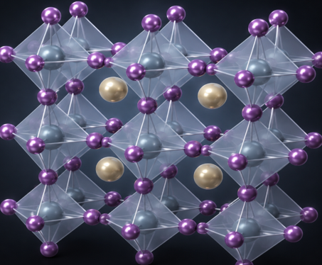

Key Materials and Technology Solutions for Perovskite Solar Cells
Perovskite solar cells (PSCs) are among the most promising next-generation photovoltaic technologies, offering high power conversion efficiency, low manufacturing cost, and exceptional design flexibility. As the technology continues to mature, PSCs are expected to play a pivotal role in the global transition toward clean, affordable, and sustainable energy.
Charge transport materials are fundamental to the performance, stability, and manufacturability of perovskite solar cells (PSCs). By selectively extracting and ransporting charge carriers while suppressing charge recombination, these functional materials directly influence power conversion efficiency, operational lifetime, and large-area device uniformity. To meet the demanding requirements of commercial manufacturing, MoleculaX develops and manufactures highperformance charge transport materials specifically engineered for industrial-scale PSC production. Our portfolio includes advanced hole and electron transport materials, interfacial passivation materials, and functional additives that enable high-efficiency, reproducible, and scalable perovskite photovoltaic technologies.
Beyond materials supply, we collaborate closely with customers and research partners through joint development programs, providing technical expertise in material selection, device architecture, process optimization, and manufacturing scale-up. By integrating innovative materials with application-driven engineering support, MoleculaX is committed to accelerating the commercialization of perovskite photovoltaic technologies and enabling the next generation of highperformance solar energy solutions.